PerfectMoney

Tuesday, December 15, 2015

Tuesday, February 24, 2015

Curtain Opener and Closer Circuit

This circuit will open and close the curtain of your home and office  just by pushing a switch. So with the help of this unique circuit, we do not need to move from one place to open and close the curtain. This circuit is used for household use, particularly for smaller doors and windows. Due to its small size and readily available components, it can be effortlessly fixed with a curtain. You can also provide power supply to the circuit with the help of adapter existing in the market.

Curtain Opener and Closer Circuit Diagram:

Curtain Opener and Closer Circuit Diagram
Circuit Diagram of Curtain Opener and Closer –ElectronicsHub.Org
Components used in this Circuit:
  • IC
  • IC1 (CD4013)
  • IC2 (ULN2003)
  • Resistor
  • R1-R4 (5.6k)
  • R6, R5 (1K)
  • C1 (. 1uf)
  • Stepper Motor

Description:

This circuit is made up of two ICs named CD4013 and ULN2003 with few more easily available components.
CD4013 IC contains two self-governing D type flip flop on a single chip which exists in one of two states that is 0 or 1 and can store information. Each module is further capable of group of  pin outs assigned as data, set, reset, clock input and a couple complementary output Q and Q Bar .

How D Type Flip Flop Works:

D type flip flop has one input referred to as D input or data input. The truth table of D type flip flop is shown below:
This is equivalent to saying that input data appear at the output, at the end of the clock pulse. Thus the transfer of data from input to output is delayed and hence delay (D) flip flop. That’s why it is used as a delay device or latch to store 1 bit binary information. In this clock (CK) input line controls the flip flop which is used to determine whether the input data is recognized or ignored. The input is normally a clock signal. If the clock input is binary high means logic 1 the data on the D line is stored in the flip flop. As long as clock line is high the normal output will simply follow or track the D input. If the CK line is low or it is binary 0 the D input line is recognized. Means the bit store in the flip flop previously retained. The D line can do anything. It will ignore if CK is low.
CD 4013 comes in 14 pin dual inline package. Before understanding the working of circuit diagram first have a look at its pin layout.
CD 4013 Pin Diagram
CD 4013 Pin Diagram – Electronics Hub
  1. Pins 1, 2, 13 and 12 are known as complimentary outputs hence both are presented as output but with inverse of each other. Like for first flip flop Q is 1 then  Q Bar will be 0. The same is also there for another set of flip flop.
  2. Pin 5 and 9 are known as Data pins they are normally connected to one of the outputs can be Q or  enlargingnction of enlargement the appsquare wavesclock for square wave and for other waves they may be ended to any other logic level means they may be either connected to supply line or to the ground of the circuit. In our circuit we have attached Q Bar and Data pin 5 as one.
  3. Pin 3 and 11 are known as Clock input. It is used to receive the input signal for working of D type flip flop. You can provide signals with the help of transistor configured as astable multivibrator or you can provide signals through logic gate like by NANA gate or NOR gate. In our circuit we are providing the clock input with the help transistor.
  4. Pin 4, 6 and 10, 8 are known as set and reset pin whenever any one of the pin goes high we will receive the output. For protection these pins are assigned to a logic level normally they are grounded with a high value resistor. Once this is completed the input can be made to alternately react to positive peak pulses to control the logic stage of the Q and Q Bar output alternately.
  5. Pin 14 and 7 are called supply and ground pin respectively. Pin 14 receives the power supply input that is Vcc which should not be more 15V otherwise it will tear down the IC and pin 7 is ground and it should be connected to the negative supply input of IC.
And ULN2003  is basically a Darlington array of high voltage as well as of high current every ULN2003 IC comprise seven unlock collector Darlington couples along with common emitter. ULN2003 is furthermore commonly used in a large variety of loads with the assist of relay drivers or may be employed  to drive a stepper motor. ULN2003 works with 5V TTL and CMOS logic devices. Each channel or else Darlington couple in ULN2003 is marked at 500mA and be able to resist peak current of 600mA.Below pin diagram of IC ULN2003 is shown:
ULN2003 Pin Diagram
ULN2003 Pin Diagram
Working on this circuit is very easy to understand. Assemble the circuit properly and cross check the connection.  In this circuit we are utilizing both the flip.
If you want to open the curtain just press switch S1 for some time. This will supply the voltage to pin 6 of IC1 (which is set pin) as one end of the switch is connected with power supply and when pin 6 goes high it will provide you the highest output at pin 1 of IC1 that is at Q output. Which in turn makes the pin 2 of IC2 also high and the geared motor connected  at the output  start revolving in the close wise direction to open the curtain. Now when the curtain is open properly or you want to stop the motor in between just press the switch S2 connected at pin 4 of IC1 which is reset pin and this is used to off or stop the stepper motor when the curtain in fully open or you want to stop in between.
A similar occurrence will happen if you want to close the curtain. Just press switch S3 for some time  connected to pin 8 of IC1 which is also a set pin. Geared motor starts running in anticlockwise direction. Now when the curtain is close or you want to stop in between  press the switch S4 to off the stepper motor. Therefore you can now open and close your curtain just by sitting in one place, without moving just by pressing the switch.

Luggage Security Alarm Project Circuit

During our journey through train and bus, we carry many important things and all the time we have fear that someone might lift our luggage. So to protect our baggage, we normally lock our baggage through old ways by the help of chain and lock. After all locks, we still remain in fear that someone may slash the chain and take away our valuable material. To overcome with these fear, here is an easy circuit which is based on the NAND gate. In this circuit, when someone tries to lift your luggage, it will generate a warning alarm which is very much helpful during your travel in the bus or train even at the night time as it can also produces audio visual indication attached to the relay.Another application of this circuit is that you can employ these into your house so to avoid the attempt of robbery in your house with the help of this alarm circuit. When anyone tries to open the door of your house, loop break down and sound from the alarm produce.

Luggage Security Alarm Circuit Diagram:

Luggage Security Alarm Circuit Diagram
Luggage Security Alarm Circuit Diagram – ElectronicsHub.Org
Circuit Components:
  • IC
    • IC1(CD4011) – 1
  • Resistor
    • R1(1K) – 1
    • R2(4.7K) – 1
  • Capacitor
    • C1(.1uF) – 1
  • Miscellaneous
    • Relay – 1
    • T1(BC547) – 1
    • D1(1N4007) – 1

Luggage Security Alarm Circuit Description:

The basic building block of this circuit is CD4011 along with some other components viz. resistors, capacitor along with transistor and relay which is used to save your important things from robbery with the help of this easy circuit. It produces a warning beep, when someone tries to unlock the lock as an effect of its wire loop will split and alarm is produced.
To get familiar with the working, you should get aware with the NAND gate truth table which is shown below -
NAND Gate - Truth Table
NAND Gate – Truth Table
When any of the input states or both the input states go to the low state in the NAND gate, then the output will be high and if both the inputs are at high state, then the output will be low in that case.
CD4011 is the mainly used CMOS (Complementary Metal Oxide Semiconductor) chip.  It arrives in a Dual Inline Package (DIP) of 14 pin. There is a small notch present on the chip at one of the corner which is recognized as pin 1. In a single chip, it is a group of 4 NAND Gate which are independent of each other. Each gate is a three terminal device with 2 terminals for the input purpose and one is for the output purpose. 5V to 16V is the working voltage range of the IC. Approximately 10mA of current at 12 V is been deliver by the IC which can be trim down with the reduction of the power supply voltage.
Related Post: Also Read the Interesting Post – Pull Pin Security Alarm System
Functioning of these circuits is very easy when we will receive; output is based on the voltage on pin 5. At the time when power supply is attached to the circuit pin 5, voltage is at zero as loop is unbroken. Hence at pin 4, voltage is high which is coupled with pin1 and pin 2 which is also at high state. As you can also find from the truth table of the NAND gate that if both the inputs are at high state, then the output is low hence at the pin 3 of gate 1, we get low which is once more attached to pin 12 as well as 13 moving them also to the low which in turn makes the pin 11 to switch at high switching pin 8 as well as pin 9 also at high and low voltage at pin 10 due to this transistor linked to it via a resistor will not boost the base of it and the alarm will not receive by us. This implies that our baggage is secure.
Now suppose that someone attempt to take your baggage then the loop attached to it broken down. At the time loop break down, pin 5 as well as pin 6 shift to high and just opposite work will take place which we will explained above due to which pin 10 reaches to high state and transistor begin its conduction and alarm is receive by us.
And the alarm will not stop till the time we once again interact with the loop. Based on the rating of the relay that you are using in your circuit value of the battery will vary in the range of 6-15V. If you wish, you can directly fix the buzzer without using relay. We are using the relay in our circuit because if anybody wants to connect the alarm directly with the AC, then also it will work without making any damage. Diode is also fixed in our circuit because if there any spikes of the reverse voltage, then it will be short-circuited at the source itself and there will be no damage done by it.

Mains Operated LED Light Circuit

Today fluorescent bulb and tube light are becoming outdated and they are replaced by LED lights as LED lights consume less power and have long life in comparison to fluorescent lamp and tube light. LED lights have many advantages over Fluorescent lamp and are mentioned at the end of this post.Here, we have described a simple circuit which you can easily made and install in your homes and will not only save resources but your energy and money will also be saved.

Mains Operated LED Light Circuit Diagram:

Mains Operated LED Circuit Diagram
Mains Operated LED Circuit Diagram – ElectronicsHub.Org
Components used in this Circuit:
  • Bridge rectifier – 1
  • Resistor
  • R1(2.M/1W) – 1
  • R2(22E/1W) – 1
  • C1(.22uF/400V) – 1
  • LED – 5

Mains Operated LED Circuit Explanation:

This simple circuit is based on Bridge rectifier, resistor, LED and capacitor. All the components used in this circuit are easily and radially available in market. So make this circuit and install in your home and offices. Before understanding the working of circuit first have a look on the component description first.
1. A rectifier is an electronic circuit used for converting an alternating current (AC) to direct current(DC). And the process of converting alternating current to direct current by allowing one way electron flow is called as rectification. In full wave rectifier four diodes are connected in a circuit to form a bride. In this we are utilizing both positive and negative of AC.
A bridge rectifier contains four diodes D1, D2, D3, D4 connected to form a bridge as shown in figure. Hence this arrangement is known as a bridge rectifier.
Bridge Connection of Diodes
Working of Bridge Rectifier:
The AC signal to be rectified is applied to the diagonally opposite ends of the bridge through the transformer. Between another two ends of the bridge, The load resistance RL is connected.
During positive half cycle of secondary voltage, The end P become positive and end Q negative. Thus Diode D1 and D3 will become forward bias and start conducting , while diode D2, D4 are reversed bias.
Diode D1 and D3 are in series with the load resistance RL hence current flows through Ras shown in figure.
D1 and D3 Series Connection with Load Resistance RL
 During negative half cycle of secondary voltage, the P end becomes negative and Q end become positive. Diode D2 and D4 are forward biased hence they start conducting . Whereas diode D1 and D3 are reversed biased.
Diode D2 and D4 are in series with the load resistor RL hence current flows through RL  as shown in figure. It may be seen that again current flows from A to B through the load i.e. in the same direction as for the positive half cycle. Thus DC voltage is obtained across load RL  . Output waveform of a bridge rectifier is shown in figure below. The advantage of Bridge rectifier is that its output is higher than of full wave and half wave rectifier.
Output waveform of a bridge rectifier
2. Light emitting diode are different  from other diodes as they emit light and hence referred as light emitting diode. LED are available in RED, GREEN, BLUE color.
3. All material have some type of opposition to the current flow. This opposition is called resistance. The resistance of a material is determine by the number of free electrons in the material. There are various type of resistor available such as carbon film, carbon composition, filament resistor and many more which can be used in an electronics or electrical circuit to determine the resistance.
Resistance of circuit depends upon p, L and A with the following equation.
R = p*(L/A)
4. The capacitor is a device that store electrical energy and capacitance is the amount of electrical energy stored at a given voltage drop by capacitor. A device specially designated to have a certain value of capacitance is called a capacitor. The capacitor has the ability to store electrons and release them at later stage. The capacitor is generally consist of two metal plate which are separated by a non conducting material called as dielectric.
5. Diode is an electronic device which allows current to flow only in one direction. Diodes are forward by joining N type and P type semiconductors. The N type semiconductor contains free electrons that move through the material. Similarly P type semiconductor contains holes. Electrons from the N type which are near the junction cross the  junction and fill in the holes in P type material. Similarly holes near the junction of  P type material, crosses the junction and occupy the place of electrons. A depletion layer is formed at the junction of the PN semiconductor.
6. Light emitting diode are different  from other diodes as they emit light and hence referred as light emitting diode. LED are available in RED, GREEN, BLUE color.
Working of circuit is very simple. Assemble the circuit properly as shown in circuit diagram. Now apply AC mains. Resistor R2  is used as current limiting components.  And resistor R1 is used with capacitor C1 so that it will discharge the capacitor which prevent lethal shock. Now this power supply is provides to bridge rectifier circuit which will convert the AC to DC and also reduces the voltage with the help of current limiting components. Now this power supply is passed to LED’s and LED connected at the output start glowing. You can use bridge rectifier available in market or you can make your own with the help of four diodes. Maximum you can use 20 LED’s.

Advantages of LED Bulbs:

  • LED bulbs have 10 times longer life in comparison  to fluorescent and incandescent lights.
  • LED bulbs does not contain filament so there is less chances of damage.
  • Common incandescent bulb become hot and generate lot of heat in the room while LED bulb prevents the heat build up and helps in reducing the air conditioning cost in room.
  • Power consumption of LED lamp is approx. 2-17 watt 1/3 in comparison to fluorescent lamp. So if you LED bulb you can save much on your electricity bill.
  • As power consumption of  LED lamp is very less, use in solar panels is increasing.
  • Many people are using inverters in their home and now they are using LED lights with inverters because this will also increase the time period for which inverters can support LED light.
  • Initial cost of LED bulb is more in comparison to fluorescent bulb with they have long life and they can be easily move from one place to another without breakage and save electricity also. Therefore LED bulb is more efficient than fluorescent bulb.
  • LED bulbs are not sensitive to temperature or humidity.
  • LED bulb does not contain mercury also hence do not provide harm to environment also.
  • LED lights will turn on instantly.

Audio Equalizer Circuit

The circuit presented here is used to change the tune/melody into a different pitch level by devoid of loss in the tune. The characteristics of the signal might be varied at different moment of time. The melody which is produced by melody generator IC can be postponed and the pitch of the tune mottled at different instance of time. This can generate different musical sounds from a single melody.The word ‘modulation’ is used to denote change of the tune by generating delay along with other effects.

Circuit Diagram of Audio Equalizer Circuit:

Audio Equalizer Circuit Diagram
Audio Equalizer Circuit Diagram – ElectronicsHub.Org
Components Used in this Circuit:
  • IC
    • IC1, IC2(4046) – 2
    • IC3(NE555) – 1
    • IC4(CD4051) – 1
  • ResistorC1,C2(4.7uf) – 2
    • R1,R3(2.2K) – 2
    • R2,R4(220K) – 2
    • R5,R6(10K) – 2
    • R7(56K) – 1
    • VR1(10K) – 1
    • VR2(5K) – 1
  • C3(470uf) – 1
  • C4(.1uf) – 1
  • D1(1N4148) – 1
  • T1(SL100) – 1
  • UM66 – 1
  • Speaker – 1

Components Description:

1. Phase Locked Loop (for Voltage Controlled Oscillator):
IC for the Phase Locked Loop is linked with 220K ohm (R2 ae well as R4) at pin number 12.The offsets are mainly provided by these resistors. Large value of R2 or R4 implies that there is a merely a minute offset.To shun total silence at the time input is 0V, R2 resistor offsets the range of frequency.
The frequency at output from VCO(pin4) at the time when voltage at pin 9 is half the voltage given is calculated by
      f=1/ (R1*C1) = 1/ (2.2K*4.7u) = 96.71 Hz.
The frequency alter with the variation of the voltage at VCO’s input is altered by potentiometer.
2. 555 Timer: This IC works like a astable multivibrator.
The on-time is = R5+C3=10Kohm*470pF=47msec
Off-time is also equal to 4.7 m sec (R6*C3)
The diode is connected to restrict the path during off-time while discharging the capacitor.The main thinking is to have the similar on and off times(50% of the duty cycle). To remove any noise presented in the circuit then C4 of 0.1uF is used.It is not compulsory to be connected.
555 timer output is worked as a selection line for the multiplexer, both the outputs of VCO is multiplexes by it.
3.Multiplexer: CD4051 is worked as 2.1 multiplexer, with both the ouput of VCO’s worked as inputs for pin 13 and 14 of MUX and a line for selection is used to select output from each of these from PLL having same time period. By concluding few additional VCO’s variety of effects can be inserted to the audio and multiplexing them and the speaker get it as an output.  Lots of varieties of UM66T are available in the market which produces tone of various songs. For example ‘Jingle bells’, we wish you a merry X’mas and ‘santa Clause is coming to town produced by the UM66T01. To alter the melodies any melody can be used in the place of UM66 in the circuit above.

Working of Audio Equalizer Circuit:

IC UM66 is used in the circuit to alter the melody which is produced by the melody generator. Oscillation is generated by the voltage controlled oscillator at the time when constant voltage is applied. For the purpose of the VCOs phase locked loop IC (i.e. 4046) which is IC1 and IC2 in the circuit is used. PLL chip comprises of VCO as well as Phase comparator.
By the help of the potentiometer, the voltage which is given to VCOs can be changed. To modify the VCO input voltage potentiometer of value 5K and 10K are attached in the circuit. This voltage is taken by IC1 and IC2. The output of VCOs at the pin 4 of IC CD4046 is a time-multiplexed by a CD4051 multiplexer IC (which IC 4 in the circuit diagram).
The signal which is selected for the multiplexer is produced by 555 timer(IC3) which is working as a astable multivibrator. 4.7 is the time taken by the each high as well as low pulse which is upcoming from 555 timer. The duty cycle is produce surely to be 50% by bringing a IN4148 a small signal diode. The output is then applied to the NPN transistor at the base terminal by a 40K ohm resistor.
The input for melody generator UM66 (Various other IC for the purpose of melody generation can also be used) is taken from the collector terminal. The output of the melody generator is then supplied at one terminal of the 4 ohm speaker(SP) and the left terminal of the speaker is linked with 5 volt power supply.
With the minute alterations in the locations of the potentiometer, the same tune can listen to the many distinct tones, height as well as pitch. In the same manner variety of  melodies can be changed by just putting that particular melody IC at the place of UM66 in the above circuit.

Air Flow Detector Circuit

Air flow detection is often necessary in many applications or systems where it is necessary to detect the presence of air to have a descriptive picture of the proper functioning of the systems. For example, we need air flow detection in engines to get an estimate about the amount of fuel to be added to the engine, we need air flow detection to check the amount of contamination or the transfer of contamination using chemical media like air. For high power density electronic devices, we need air flow detection to ensure the devices from getting over heated.

Principle Behind Air Flow Detector Circuit:

Here, a simple air flow detector circuit is developed which uses a resistance temperature detector as the basic component. This circuit is based on two principles – a) Variation of resistance with temperature, b) Air as an insulator.  As current flows through the resistor, it gets heated up. Now when air is made to flow through the RTD, it being an insulator, allows the resistor to cool down. Thus resistance starts decreasing and the voltage across the RTD decreases. This variation in voltage drop is detected using a timer circuit to give an indication of the air flow.

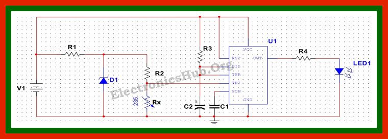
Air Flow Detector Circuit Diagram:

Air Flow Detector Circuit Diagram
Air Flow Detector Circuit Diagram – ElectronicsHub.Org
Circuit Components:
  • V1 = 12 V
  • R1 = 38 Ohms
  • D1= 4.7 V Zener diode, 1N4732
  • R2 = 100 Ohms
  • Rx = HEL-700 platinum RTD
  • R3 = 10K
  • C2 = 1uF
  • C1= 0.01 uF
  • LED = 5V, Green LED
  • IC = 555 Timer

Air Flow Detection Circuit Design:

This circuit is designed to provide a constant current input to the RTD so that it is heated slightly at the beginning. The RTD selected here is HEL-700 platinum RTD, which works at a maximum operating current of 2 mA. Here we are using a Zener Diode as a voltage regulator to provide a constant current to the RTD.
To design a Zener voltage regulator, we need to first select the Zener diode. Here a Zener diode with Vz = 4.7V is selected. Since input voltage is 12V and required output current is 2mA, we select a load resistance of 100 Ohms, so that maximum current flows through the load and only a small amount of current flows through the RTD. The input resistance selected is given by (Vin-Vz)/(Iz+IL) and is equal to 38 Ohms. Here a 38 Ohms resistor is used as the input resistor.
The next step requires design of timer monostable multi vibrator. Here the timer is used to provide biasing voltage to the LED, which is about 5V. The LED is required to glow as the voltage across the RTD decreases. Here we select a resistor of 10K and an electrolyte capacitor of 1uF.  A ceramic capacitor of 0.01uF is used to connect the control pin to ground.

Air Flow Detector Circuit Operation:

This circuit is operated using a 12V battery. The battery voltage is regulated using the Zener diode, which produces a constant voltage. Initially as current flows through the RTD, it gets heated up and its temperature increases, thereby increasing its resistance.  Now as current is constant, the voltage across the resistance also tends to increase.  When this voltage is applied to the trigger pin of the timer, it fails to trigger the timer and the LED is in off condition. Now as air flows over the RTD, it starts cooling. This reduces the temperature of the device. As the temperature reduces, the resistance also reduces and so does the voltage across the device. As this voltage reduces below a certain point, the timer gets triggered and the LED starts blinking. As voltage falls further, indicating fall of temperature, the LED starts glowing with full intensity. This indicates the flow the air.

Theory Behind Air Flow Detector Circuit:

The basic theory behind this circuit involves knowledge about three basic parts- Voltage Regulator using Zener Diode, Resistance Temperature detector and a timer circuit.
Voltage Regulator using Zener Diode:
Zener diode is a simple PN junction diode operated in reverse bias condition. It basically works on the principle of breakdown – Avalanche and Zener. Zener breakdown occurs at a reverse bias voltage between 2V to 8V, when highly strong electric field intensity causes the electrons to break free from the atoms and form free electron hole pairs. The avalanche breakdown occurs above 8V, when high speed charge carriers cause disrupt of covalent bond due to collision, leading to formation of free electrons.
As can be seen by the characteristics, for a large variation in current through the diode, the voltage across the diode remains very small or constant. This unique feature is utilized in many applications by using Zener diode as the voltage regulator.
Resistance Temperature Detector:
A resistance temperature detector or RTD is a metal resistor whose resistance changes with temperature. It is based on the fact that in metals, as temperature increases, the lattice vibrations increases. These vibrations cause collision among the electrons. As collisions increase, the energy of the electrons decrease, causing a decrease in the flow of free electrons, leading to low conductivity. Thus, with increase in temperature, the resistance increases. An RTD is constructed basically using platinum. At 0 degree Celsius, resistance of an RTD is about 100 Ohms.
555 Timer Multivibrator:
Multivibrator circuit is used to produce pulsed output signal. It is triggered when a low level signal is applied to the trigger pin of the IC. The 555 timer IC is an 8 pin IC and the timing of the output signal is given by T=1.1 RC. To get detailed information about 555 timer IC, read the post Understanding 555 Timer

Applications of Air Flow Detector Circuit:

This circuit can be used to detect the flow of air in areas like car engine, where it is required to estimate the amount of fuel needed by the engine. Apart from being used as an air flow detector, this circuit can also find its application as a temperature detector circuit. With slight modifications, this circuit can be used to control loads like a fan, based on temperature sensing.

Limitations of Air Flow Detector Circuit:

  1. Since Zener diode is being used, the efficiency of the circuit is affected. This is because loss in series resistor causes a decline in efficiency in case of heavy loads.
  2. The resistance temperature detector used is expensive and easily affected by shock and vibration.

Bike Turning Signal Circuit

We know the use of bike indicators. These are used to indicate left turn or right turn. Have you ever tried to design bike turning indicators. This article explains you how to design these bike turning indicators.

Bike Turning Signal Circuit Principle:

The objective of this circuit is to indicate left or right turn for bike/vehicle. Two identical circuits are needed, one is for left and the other is for right. The main heart of this circuit is 555 timer. Here, this 555 timer acts as an astable multi vibrator. It generates the pulse signal with variable width. Using this variable width of the pulse, we can set different time delays for the LEDs (ON and OFF for LEDs).
The circuit consists of two 47k resistors, which are connected to 555 timer and these are used to set the time delay for LEDs. 1n4148 signal diode is connected in reverse bias at the output to maintain constant current at the output. BC547 (NPN) Transistor switches the LED’s ON and OFF based on the base currents. 330 ohm resistors are used to drop the voltage otherwise LEDs may get damaged. Here we can vary the time width of output pulse by varying the resistance or capacitance value.

Bike Turning Signal Circuit Diagram:

Bike Turning Signal Circuit Diagram
Circuit Components:
  • Resistors       –  3 (47 k ohm)
  • Resistors       –  5 (10 k ohm)
  • Resistors       -5 (330 ohm)
  • Capacitors    – 2 (100uF)
  • Transistors   – 5 (BC547)
  • LED’s              – 10 (5 mm)
  • IC                    – 1 (NE555)
  • Diodes           – 2 (1n4148)
  • Battery          – 1 (12V)
  • wires

Bike Turning Signal Indicator Circuit Design:

In this circuit, 555 timer produces pulse signal with variable width. The pulse width is varied by varying resistance or capacitance value (R2, R1). 2 and 6 pins are shorted to allow triggering after every timing cycle. Fourth pin is reset, it is shorted with VCC (8th pin) to avoid sudden resets. 7th pin is discharging pin, it is connected to 6th pin through a 47k resistor. The below figure explains you the operation of 555 timerhttp://subjecteee.blogspot.in/. In this circuit capacitor C charges through resistors Ra and Rb. Now because of internal op-amps, capacitor C discharges through resistor Rb. 555 timer internally consist of 2 operational amplifiers, one D flip flop and one NPN transistor.
555 Timer in Astable Modehttp://subjecteee.blogspot.in/
555 Timer in Astable Mode
In the above circuit, the pulse is generated at the 3rd pin of the 555 timer. By varying the values of Ra, Rb, C we can vary the pulse width. The total time period of the pulse is given as
T = THIGH + TLOW = 0.693 (RA+ 2RB) C
 Frequency of the pulse is given as
f = 1/T = 1.44/ (RA+ 2RB)C
percentage of duty cycle is given as
% duty cycle, D = t/ T * 100 = (RA + RB) / (RA + 2RB) * 100
The obtained pulse from the 555 timer is applied to the transistors to switch the LEDs ON and OFF with some delay. Here the operating voltage of LEDs is around 2 to 3v but from battery, we get 12v supply. So, we need to drop the remaining voltage. To drop this voltage, we are using resistors in series with LEDs. 

How to Operate the Circuit?

  • Initially feed 12v power supply to the circuit.
  • Now observe the LED’s they will glow with some delay.
  • If you want, set the different time delays for LEDs, and then vary the resistance or capacitance value.
  • Now you can see the change in time delay.
  • By varying the capacitance value also you can see the in time delay of LEDs.

    Applications of Bike Turning Signal Indicator Circuit: