Introduction
Diodes are electronic components functions as a one-way valve it means it allow current to flow in one direction. These diodes are manufactured by the semiconductor materials germanium, silicon and selenium. Operation of diode can be classified in two ways, if it allows the current then it is forward biased otherwise it is reverse biased. For silicon diodes the forward voltage is 0.7v and for germanium it is 0.3v. In silicon diode the dark band indicates the cathode terminal and the other terminal is anode. Generally diodes are used as reverse polarity protector and transient protector. There are many types of diodes and some of these are listed as follows.1. Small Signal Diode
It is a small device with disproportional characteristics and whose applications are mainly involved at high frequency and very low currents devices such as radios and televisions etc. To protect the diode from contamination it is enveloped with a glass so it is also named as Glass Passivated Diode which is extensively used as 1N4148. The appearance of signal diode is very small when compared with the power diode. To indicate the cathode terminal one edge is marked with black or red in color. For the applications at high frequencies the performance of the small signal diode is very effective. With respect to the functional frequencies of the signal diode the carrying capacity of the current and power are very low which are maximum nearly at 150mA and 500mW.The signal diode is a silicon doped semiconductor diode or a germanium doped diode but depending up on the doping material the characteristics of the diode varies. In signal diode the characteristics of the silicon doped diode is approximately opposite to the germanium doped diode. The silicon signal diode has high voltage drop at the coupling about 0.6 to 0.7 volts so, it has very high resistance but low forward resistance. On other hand germanium signal diode has low resistance due to low voltage drop nearly at 0.2 to 0.3 volts and high forward resistance. Due to small signal the functional point is not disrupted in small signal diode.
2. Large Signal Diode
These diodes have large PN junction layer. Thus the transformation of AC to DC voltages is unbounded. This also increases the current forward capacity and reverse blocking voltage. These large signals will disrupt the functional point also. Due to this it is not suitable for high frequency applications. The main applications of these diodes are in battery charging devices like inverters. In these diodes the range of forward resistance is in Ohms and the reverse blocking resistance is in mega Ohms. Since it has high current and voltage performance these can be used in electrical devices which are used to suppress high peak voltages.3. Zener Diode
It is a passive element works under the principle of zener breakdown. First produced by Clarence zener in 1934.It is similar to normal diode in forward direction, it also allows current in reverse direction when the applied voltage reaches the breakdown voltage. It is designed to prevent the other semiconductor devices from momentary voltage pulses. It acts as voltage regulator.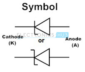
4. Light Emitting Diode (LED)
These diodes convert the electrical energy in to light energy. First production started in 1968. It undergoes electroluminescence process in which holes and electrons are recombined to produce energy in the form of light in forward bias condition. Earlier they used in inductor lamps but now in recent applications they are using in environmental and task handling. Mostly used in applications like aviation lighting, traffic signals, camera flashes.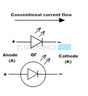
5. Constant Current Diodes
It is also known as current-regulating diode or constant current diode or current-limiting diode or diode-connected transistor. The function of the diode is regulating the voltage at a particular current. It functions as a two terminal current limiter. In this JFET acts as current limiter to achieve high output impedance. The constant current diode symbol is shown below.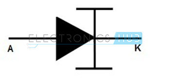
6. Schottky Diode
In this type of diode the junction is formed by contacting the semiconductor material with metal. Due to this the forward voltage drop is decreased to min. The semiconductor material is N-type silicon which acts as an anode and the metal acts as a cathode whose materials are chromium, platinum, tungsten etc. Due to the metal junction these diodes have high current conducting capability thus the switching time reduces. So, Schottky has greater use in switching applications. Mainly because of the metal- semiconductor junction the voltage drop is low which in turn increase the diode performance and reduces power loss. So, these are used in high frequency rectifier applications. The symbol of Schottky diode is as shown below.
7. Shockley Diode
It was the invention of first semiconductor devices it has four layers. It is also called as pnpn diode. It is equal to a thyristor without a gate terminal which means the gate terminal is disconnected. As there is no trigger inputs the only way the diode can conduct is by providing forward voltage. It stays on one’s it turned “ON” and stays off one’s it turned “OFF”. The diode has two operating states conducting and non-conducting. In non-conducting state the diode conducts with less voltage.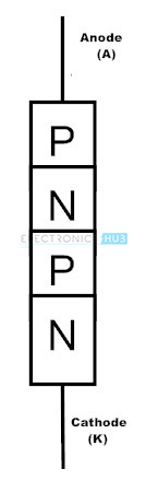
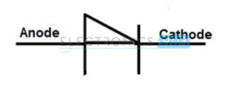
The symbol of the Shockley diode is as follows:
Shockley Diode Applications:
- Trigger switches for SCR.
- Acts as relaxation oscillator.
8. Step Recovery Diodes:
It is also called as snap-off diode or charge-storage diode. These are the special type of diodes which stores the charge from positive pulse and uses in the negative pulse of the sinusoidal signals. The rise time of the current pulse is equal to the snap time. Due to this phenomenon it has speed recovery pulses. The applications of these diodes are in higher order multipliers and in pulse shaper circuits. The cut-off frequency of these diodes is very high which are nearly at Giga hertz order. As multiplier this diode has the cut-off frequency range of 200 to 300 GHz. In the operations which are performing at 10GHz range these diodes plays a vital role. The efficiency is high for lower order multipliers. The symbol for this diode is as shown below.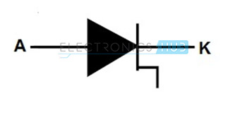
9. Tunnel Diode
It is used as high speed switch, of order nano-seconds. Due to tunneling effect it has very fast operation in microwave frequency region. It is a two terminal device in which concentration of dopants is too high. The transient response is being limited by junction capacitance plus stray wiring capacitance. Mostly used in microwave oscillators and amplifiers. It acts as most negative conductance device. Tunnel diodes can be tuned in both mechanically and electrically. The symbol of tunnel diode is as shown below.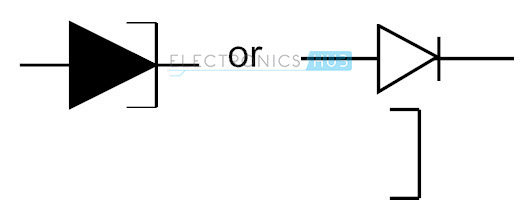
Tunnel Diode Applications:
- Oscillatory circuits.
- Microwave circuits.
- Resistant to nuclear radiation.
10. Varactor Diode
These are also known as Varicap diodes. It acts like the variable capacitor. Operations are performed mainly at reverse bias state only. These diodes are very famous due to its capability of changing the capacitance ranges within the circuit in the presence of constant voltage flow. They can able to vary capacitance up to high values. In varactor diode by changing the reverse bias voltage we can decrease or increase the depletion layer. These diodes have many applications as voltage controlled oscillator for cell phones, satellite pre-filters etc. The symbol of varactor diode is given below.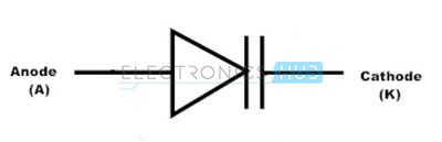
Varactor Diode Applications:
- Voltage-controlled capacitors.
- Voltage-controlled oscillators.
- Parametric amplifiers.
- Frequency multipliers.
- FM transmitters and Phase locked loops in radio, television sets and cellular telephone.
11. Laser Diode
Similar to LED in which active region is formed by p-n junction. Electrically laser diode is p-i-n diode in which the active region is in intrinsic region. Used in fiber optic communications, barcodereaders, laser pointers, CD/DVD/Blu-ray reading and recording, Laser printing.Laser Diode Types:
- Double Heterostructure Laser: Free electrons and holes available simultaneously in the region.
- Quantum Well Lasers: lasers having more than one quantum well are called multi quantum well lasers.
- Quantum Cascade Lasers: These are heterojunction lasers which enables laser action at relatively long wavelengths.
- Separate Confinement Heterostructure Lasers: To compensate the thin layer problem in quantum lasers we go for separate confinement heterostructure lasers.
- Distributed Bragg Reflector Lasers: It can be edge emitting lasers or VCSELS.
12. Transient Voltage Suppression Diode
In semiconductor devices due to the sudden change in the state voltage transients will occur. They will damage the device output response. To overcome this problem voltage suppression diode diodes are used. The operation of voltage suppression diode is similar to Zener diode operation. The operation of these diodes is normal as p-n junction diodes but at the time of transient voltage its operation changes. In normal condition the impedance of the diode is high. When any transient voltage occurs in the circuit the diode enters in to the avalanche breakdown region in which the low impedance is provided. It is spontaneously very fast because the avalanche breakdown duration ranges in Pico seconds. Transient voltage suppression diode will clamp the voltage to the fixed levels, mostly its clamping voltage is in minimum range. These are having applications in the telecommunication fields, medical, microprocessors and signal processing. It responds to over voltages faster than varistors or gas discharge tubes.The symbol for Transient voltage suppression diode is as shown below.

The diode is characterized by
- Leakage current
- Maximum reverse stand-off voltage
- Breakdown voltage
- Clamping voltage
- Parasitic capacitience
- Parasitic inductance
- Amount of energy it can absorb
13. Gold Doped Diodes
In these diodes gold is used as a dopant. These diodes are faster than other diodes. In these diodes the leakage current in reverse bias condition also less. Even at the higher voltage drop it allows the diode to operate in signal frequencies. In these diodes gold helps for the faster recombination of minority carriers.14. Super Barrier Diodes
It is a rectifier diode having low forward voltage drop as schottky diode with surge handling capability and low reverse leakage current as p-n junction diode. It was designed for highpower, fast switching and low-loss applications. Super barrier rectifiers are the next generation rectifiers with low forward voltage than schottky diode.15. Peltier Diode
In this type of diode, at the two material junction of a semiconductor it generates a heat which flows from one terminal to another terminal. This flow is done in only single direction that is as equal to the direction of current flow. This heat is produced due to electric charge produced by the recombination of minority charge carriers. This is mainly used in cooling and heating applications. This type of diodes used as sensor and heat engine for thermo electric cooling.16. Crystal Diode:
This is also known as Cat’s whisker which is a type of point contact diode. Its operation depends on the pressure of contact between semiconductor crystal and point. In this a metal wire is present which is pressed against the semiconductor crystal. In this the semiconductor crystal acts as cathode and metal wire acts as anode. These diodes are obsolete in nature. Mainly used in microwave receivers and detectors.Crystal Diode Applications:
- Crystal diode rectifier
- Crystal diode detector
- Crystal radio receiver
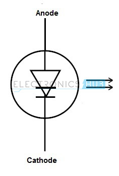
17. Avalanche Diode:
This is passive element works under principle of avalanche breakdown. It works in reverse bias condition. It results large currents due to the ionization produced by p-n junction during reverse bias condition. These diodes are specially designed to undergo breakdown at specific reverse voltage to prevent the damage. The symbol of the avalanche diode is as shown below: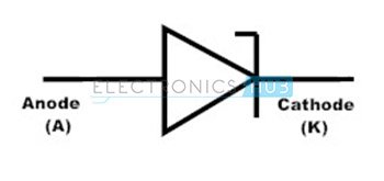
Avalanche Diode Uses:
- RF Noise Generation: It acts as source of RF for antenna analyzer bridges and also as white noise generators. Used in radio equipments and also in hardware random number generators.
- Microwave Frequency Generation: In this the diode acts as negative resistance device.
- Single Photon Avalanche Detector: These are high gain photon detectors used in light level applications.
18. Silicon Controlled Rectifier
It consists of three terminals they are anode, cathode and a gate. It is nearly equal to the Shockley diode. As its name indicates it is mainly used for the control purpose when small voltages are applied in the circuit. The symbol of the Silicon Controlled Rectifier is as shown below: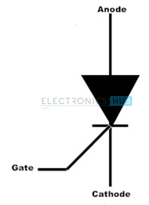
Modes of Operation:
- Forward blocking mode (off state): In this j1 and j3 forward biased and j2 is reverse biased. It offers high resistance below breakover voltage and hence it is said to be off state.
- Forward conduction mode (on state): By increasing the voltage at anode and cathode or by applying positive pulse at the gate we can turn ON. To turn off the only way is to decrease the current flowing through it.
- Reverse blocking mode (off state): SCR blocking the reverse voltage is named as asymmetrical SCR. Mostly used in current source inverters.
19. Vacuum Diodes
Vacuum diodes consist of two electrodes which will acts as an anode and the cathode. Cathode is made up of tungsten which emits the electrons in the direction of anode. Always electron flow will be from cathode to anode only. So, it acts like a switch. If the cathode is coated with oxide material then the electrons emission capability is high. Anode is a bit long in size and in some cases their surface is rough to reduce the temperatures developing in the diode. The diode will conduct in only one case that is when the anode is positive regarding to cathode terminal. The symbol is as shown in figure: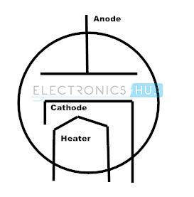
20. PIN Diode
The improved version of the normal P-N junction diode gives the PIN diode. In PIN diode doping is not necessary. The intrinsic material means the material which has no charge carriers is inserted between the P and N regions which increase the area of depletion layer. When we apply forward bias voltage the holes and electrons will pushed into the intrinsic layer. At some point due to this high injection level the electric field will conduct through the intrinsic material also. This field made the carriers to flow from two regions. The symbol of PIN diode is as shown below: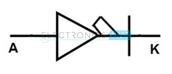
PIN Diode Applications:
- Rf Switches: Pin diode is used for both signal and component selection. For example pin diodes acts as range-switch inductors in low phase noise oscillators.
- Attenuators: it is used as bridge and shunt resistance in bridge-T attenuator.
- Photo Detectors: it detects x-ray and gamma ray photons.
21. Point Contact Devices
A gold or tungsten wire is used to act as the point contact to produce a PN junction region by passing a high electric current through it. A small region of PN junction is produced around the edge of the wire which is connected to the metal plate which is as shown in the figure.
In forward direction its operation is quite similar but in reverse bias condition the wire acts like an insulator. Since this insulator is between the plates the diode acts as a capacitor. In general the capacitor blocks the DC currents when the AC currents are flowing in the circuit at high frequencies. So, these are used to detect the high frequency signals.
22. Gunn Diode
Gunn diode is fabricated with n-type semiconductor material only. The depletion region of two N-type materials is very thin. When voltage increases in the circuit the current also increases. After certain level of voltage the current will exponentially decrease thus this exhibits the negative differential resistance. It has two electrodes with Gallium Arsenide and Indium Phosphide due to these it has negative differential resistance. It is also termed as transferred electron device. It produces micro wave RF signals so it is mainly used in Microwave RF devices. It can also use as an amplifier. The symbol of Gunn diode is shown below: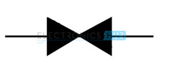
No comments:
Post a Comment
some simple projects for Electrical&Electronics students